
@typecad/pcb
v1.0.0-alpha.9
Published
🤖programmatically 💥create 🛰️hardware
Downloads
968

Maintainers
 typecad0
Readme
typeCAD/pcb
🤖 programmatically 💥 create 🛰️ hardware
typeCAD is a way to programmatically create hardware designs — KiCAD + TypeScript + npm. @typecad/pcb is the core package: schematics, PCB layout, placement, autorouting, zones, stitching, simulation, KiCad project import, native ERC/DRC checks, multi-board projects, and a built-in gerber board viewer, with passives built in.
It's done with TypeScript and all the awesomeness of the npm/Node.js ecosystem.
- npm packages can be imported into your projects
- create portable/importable/shareable packages
- semantic version control
The schematic portion of hardware design is replaced with a few simple TypeScript classes. Rather than clicking and dragging, a line of code creates a component, and another line connects it. Sections of code can be turned into reusable modules and those modules can be turned into npm packages.
Code can be version controlled, status tracked, git push/pull/PR/issues can be used, and all the typical tools for software design can be used for hardware design now
Example
This typeCAD code...
import { Component, PCB, Resistor, LED } from '@typecad/pcb'

let typecad = new PCB('typecad');
let bt1 = new Component({ footprint: 'Battery:BatteryHolder_Keystone_500' });
let r1 = new Resistor({ value: '1 kOhm', size: '0805' });
let d1 = new LED();

typecad.named('vin').net(bt1.pin(1), r1.pin(1));
typecad.net(r1.pin(2), d1.pin(2));
typecad.named('gnd').net(d1.pin(1), bt1.pin(2));

typecad.create(r1, d1, bt1);
...is the same as this schematic.
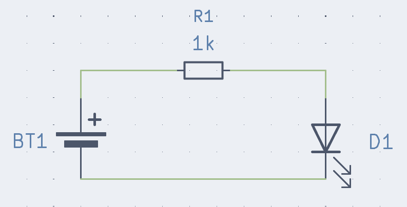
The difference is that code can be copied, turned into reusable packages, version controlled, and used within the npm/Node.js system.
Passives
Resistors, capacitors, inductors, diodes, LEDs, and fuses are built in — no second package. The SMD package size is a constructor option (default 0603), and an explicit footprint always wins:
import { PCB, Resistor, Capacitor, Connector, TestPoint, MountingHole, NetTie } from '@typecad/pcb'

let r1 = new Resistor({ value: '4.7 kOhm' });                 // 0603 (default)
let r2 = new Resistor({ value: '10 kOhm', size: '0805' });    // explicit size
let c1 = new Capacitor({ value: '100 nF', voltage: '6.3 V' });
let j1 = new Connector({ number: 4, series: 'JST-SH' });      // footprint templated from the pin count
Sizes: '0201' | '0402' | '0603' | '0805' | '1206' | '1210' (fuses from '0603' up). Inside a Package, this.passives.Capacitor(...) works out of the box; shift a whole package with { passiveSize: '0805' }.
Get started
Read through the documentation for a full walkthrough:
npx @typecad/pcb createCommand line
Everything is driven by the typecad-pcb CLI — the package also installs pcb, gerber-viewer, kicad-symbols, and kicad2typecad bins. npx @typecad/pcb create scaffolds a project with npm scripts wired up (npm run build → typecad-pcb build, npm run kicad_sync → watch-mode import, ...):
| Command | What it does |
| --- | --- |
| create | create a new typeCAD project |
| add component / add package | add a component to the project / create a reusable component package |
| build | build KiCAD output from typeCAD source |
| clean | remove the generated build directory |
| check | build + ERC + DRC in one pass, one report |
| erc / drc | electrical rules / design rule checks on their own |
| diagnostics | full design report — BOM, nets, graphs, ERC/DRC (markdown) |
| query | inspect the compiled board (nets, pins, placement) |
| edit | checked semantic edits (connect, move) |
| search | search KiCad symbols and footprints |
| import | convert a KiCad PCB file to typeCAD code |
| diff | compare two KiCad PCB files visually |
| doc | generate PCB documentation from markdown |
| lib add / lib list | fetch/list KiCad libraries into build/lib |
| export gerbers / export drill | export fabrication outputs |
| validate | validate project source without a full build |
| doctor | check your environment for common issues |
| package | browse and install typeCAD packages from npm |
| skills | list and query typeCAD skills and API patterns |
Every command takes --json for machine-readable output and --help for details.
Checks without a KiCad install
ERC and DRC run on a native engine — the build computes them from the design itself, and check rolls build + ERC + DRC into one report. The legacy kicad-cli checks remain available with --kicad. lib add fetches symbol/footprint libraries into build/lib, so search and build work on machines without KiCad installed.
KiCad import
Existing boards come across with typecad-pcb import <board>.kicad_pcb — placement, nets, tracks and zones become typeCAD code. With --watch --auto (the scaffold wires this up as npm run kicad_sync) the KiCad file and the typeCAD source stay in sync while you work in either.
Multi-board projects
A project can carry more than one board — mother/daughter, board/jig. Every new PCB('<name>') the build produces gets its own build/<name>.kicad_pcb, recorded in a build manifest; --board <name> targets one board of the set, and commands default to the active (most recent) board.
Board viewer
This package ships a built-in, zero-dependency Gerber (RS-274X) + Excellon viewer:
# one-shot: render a fab-output directory to a self-contained interactive HTML file
npx gerber-viewer gerbers/ -o board-view.html --open
A ruler button in the toolbar arms a measurement mode: click a start point, move the mouse to
see the live distance, click again to stick the ruler — measurements accumulate, and Esc
clears them all. Hold Shift while measuring to snap the endpoint to 0/45/90-degree angles.
Rulers scale and pan with the board, keep a constant on-screen size while
zooming, and follow the dark/light theme.
The viewer also understands what it is showing: KiCad's X2 object attributes (%TO.N net,
%TO.P component/pin) are parsed, so hovering copper shows the net and pad in the readout,
and clicking highlights the whole net (pad→net comes from the project netlist, passed with
--netlist). A search box locates components — type U3, press Enter, and the view zooms to
its pads. A collapsible fab report panel lists board dimensions, per-layer trace lengths and
min/max widths, and the drill table. DRC violations from the build's _drc.json are drawn as
red markers when passed with --drc (hover for the message, toggle with the DRC button).
The SVG/PNG buttons export the current view — theme, layer visibility and highlight
included — as a vector file or a ~1600-pixel raster image.
Programmatic use (parsing, layer detection, SVG rendering):
import {
  parseGerber, parseExcellon, detectLayer, renderSvg,
  buildViewerFromFiles,
} from '@typecad/pcb/gerber-viewer';
PCBA image render
The same gerbers can be rendered as a flat, themed 2D "assembled board" image — the
PcbDraw look, computed from gerbers alone (no board file, no KiCad install, no
lighting or perspective). The substrate is the stitched Edge.Cuts outline, the
soldermask film is composited over copper with its openings punched through an SVG
mask so pads show in the finish color, copper traces and pours ghost through the
film in a darker mask tone (maskCopper theme color — real mask is translucent),
and components are stylized Fritzing-style glyphs (body, metal leads, pin-1 dot,
DIP notch) inferred from the X2 %TO.P pad attributes — no part library needed:
npx gerber-viewer gerbers/ --render pcba -o board-pcba.svg
npx gerber-viewer gerbers/ --render pcba --style blueprint -o board-drawing.svg
A sibling netlist is picked up automatically when it sits next to the gerber
directory (the typeCAD build layout: build/gerbers + build/<board>.net) — pass
--netlist to point at one explicitly, or --no-netlist to render from pad
topology alone.
With a KiCad netlist (--netlist, the same flag the viewer uses), each ref's
footprint name and value select the glyph: names map to a package grammar —
chips (R_0603_1608Metric renders the real 1.6 × 0.8 mm body), SOIC/TSSOP,
DIPs with a notch, QFN/DFN and BGA, QFP, SOT/TO transistors with tabs, pin
headers, terminal blocks with screw dots, shrouded connectors (USB, barrel
jacks, JST), crystals, metal-can modules (oscillators, RF shields), trimmer
pots, slide switches, rotary encoders, radial electrolytic cans, TH LED domes,
pushbuttons — and pad topology classifies anything the name table doesn't
know, with reference prefixes picking up the slack (an RV on three TH pads
is a trimmer, an LED on two is a dome). When the fab gerber
(F_Fab/B_Fab) is in the set, the exact body dimensions come from there: the
largest closed fab contour per component supplies the body rectangle (orientation
cuts like QFN pin-1 chamfers are squared off — the pin-1 dot marks orientation),
so land-pattern pads peek past the package exactly as on the real part. The
reference prefix and value then choose the appearance: through-hole resistors
get the classic tan body with real color bands ("10k" → brown black orange +
gold), MLCCs render beige, inductors charcoal with winding stripes, diodes
carry a cathode stripe, LEDs a translucent tint. Without a netlist everything
still renders from pad geometry alone, just without exact body dims and
decorations.
Themes are a small PcbDraw-style palette (green-enig — the classic green
default, plus typecad — the house look: deep teal mask, champagne-gold
pads — purple-enig, black-hasl, blue-enig) or your own JSON (--theme my-theme.json overrides any subset of the
colors, including maskCopper). Refdes labels default to auto: off when the
silkscreen layer already carries them (a synthetic label would double the silk
text — and the board's own text renders faithfully since KiCad vectorizes fonts
like OCR A Std into the gerber), on when there is none — --labels/--no-labels
forces either way. Synthetic labels use the theme's labelFont
('OCR A Std', 'Courier New', monospace by default) to match typeCAD boards.
Every render carries an engineering title block below the board — name, date,
dimensions, and a "made with typeCAD" wordmark; --no-title-block renders a
clean image. --style blueprint draws the board as an engineering drawing
instead of an assembled render: blueprint paper, board
and component outlines in ink, outlined pads, drill marks, and the title block in
drawing ink; designators come from the fab layer (synthetic labels only without one).
A combo box under the board title switches between Gerber view (the classic per-layer stack with visibility/opacity controls), PCBA view (the flat assembled render described above), and Blueprint view (the engineering drawing). All views share one coordinate frame, so pan/zoom, the measurement ruler, DRC markers, component search and the vscode cross-probing (double-click a component to jump to its source line; select one in the editor to highlight it here) all work in either view. The PCBA view hides the layer controls — there is only one layer stack to show — and the choice is remembered per board.
Inside VS Code, the bundled typeCAD/pcb extension renders this viewer (gerbers + netlist + DRC) in a Board panel that refreshes on every npm run build and cross-probes both ways with the source — see the package docs. Layer visibility and opacity settings persist across rebuilds — they're stored in your browser (localStorage, keyed per board) and re-applied when the page reloads. A dark/light theme toggle sits in the sidebar header; the theme (including the board canvas) is saved per browser and follows your OS preference on first visit. On the dark canvas, near-black layer colors (silkscreen, paste, drill) are automatically recolored so they stay visible, and clear-polarity cutouts follow the canvas color.